
Reliability
Power modules, semiconductor devices for electrical use, were launched on the market in the late 1970s as BIP type modules (transistors, thyristors, etc.) embedded in bipolar-type semiconductor chips and again in the early 1980s as MOS-type modules (IGBT etc.) embedded in MOS-type semiconductor chips. Currently they are widely used in many home electric appliances such as air-conditioners, refrigerators, washing machines, etc., and in applications for various industrial inverter devices, servo, UPS, electric and electronic peripherals.
At the same time, the reliability of the device has increased rapidly along with improvements in semiconductor technology. Typically, for equipment that demands high reliability, a semiconductor device failure rate of 10 to 100 FIT (1 FIT = 1×10⁻⁹/hour) is required. In order to realize that level of reliability, naturally the reliability of the semiconductor must be improved. It is very important to consider the harmony of the equipment design and working conditions under the various new stresses added to the semiconductor’s characteristics and reliability.
It is often observed that the failure rate in the market place is markedly different for semiconductor devices manufactured in the same way because of a weakness in machine design or a difference in usage.
Here we introduce our company’s reliability test results and activities to guarantee quality with regard to semiconductor device reliability, by examining problems of typical machine design and usage that must be take into consideration and cases of faults that actually reached the market.
2.1 Change in failure rates of semiconductor devices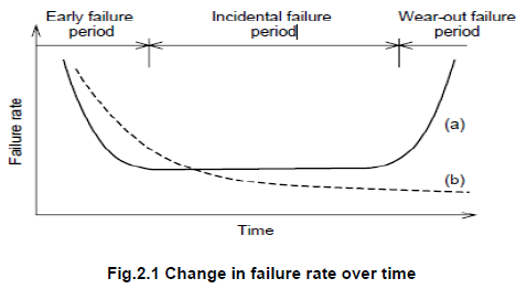
The failure rate of electrical equipment and parts follows the so-called bathtub curve shape shown in Fig. 2.1 (a), where after an early failure period, it passes through an incidental failure period before reaching wear-out failure. From this failure-rate curve, the selection of a semiconductor device for use in equipment has to consider these three points: early failure period failure rate, incidental failure period failure rate, and usable life period, in addition to the equipment use, influence and spread of faults in the device, and the preventive maintenance system, etc.
In general, the failure-rate curve of semiconductor devices resembles Fig. 2.1 (b) and tends to decrease over time.
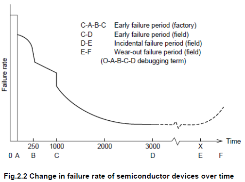
Changing the way of looking at this, even when the failure rate lowers in the incidental occurrence fault period and becomes stable, from the fault distribution pattern it can be said that the early failure shape continues. The change of the failure rate over time of the semiconductor device is shown in Fig. 2.2, and while a high failure rate is shown after manufacture, by edging and debugging the failure rate decreases further. For semiconductor devices that require high reliability, high-temperature edging and electrical edging are used for edging and debugging.
Because the failure rate curve of semiconductor devices shows a declining variation pattern, to increase the reliability of the equipment it is necessary to consider the minor initial-failure factors (especially major failure rates such as disconnects, shorts, etc.). Next, while it goes into assembly conditioning and edging with equipment maker, the major failure rate is ≤ 0.1%. If the rate dramatically exceeds this value, there is a problem in the device, circuit design, assembly process or test process and a study of the cause is necessary. If this is left, it can show up in frequent fault occurrences in the market. Caution is necessary when the failure rate is high, as there are many cases when there is a correlation between the assembly-conditioning and edging- period failure rates and market failure rate. The failure rate for heavy faults within a certain period is ≤ 0.1%. When the equipment comes on the market, the failure rate decreases dramatically because the stress level declines, and it is usually between several FIT and several 100 FIT. Because of this, design with some leeway on the device-use side is required, and generally it is desirable to have a maximum voltage rating of below 50~60%, and a maximum junction temperature rating of below 70~80%. One other important element that must be remembered is the semiconductor device in use, the circuitry used and the environmental conditions (various cases of stress, etc.), which can affect improvements in reliability too.
As stated above, when it comes to equipment reliability design, it is necessary to consider the trade-off between performance/ reliability and economy when selecting a device. It is not easy to attain both high performance/high reliability and economy, so a balance of both must be selected. It can be said that selecting a semiconductor device by considering the performance, reliability and harmony of the equipment is an important learning activity for the user.
In general, the failure-rate curve of semiconductor devices resembles Fig. 2.1 (b) and tends to decrease over time.
Changing the way of looking at this, even when the failure rate lowers in the incidental occurrence fault period and becomes stable, from the fault distribution pattern it can be said that the early failure shape continues. The change of the failure rate over time of the semiconductor device is shown in Fig. 2.2, and while a high failure rate is shown after manufacture, by edging and debugging the failure rate decreases further. For semiconductor devices that require high reliability, high-temperature edging and electrical edging are used for edging and debugging.
Because the failure rate curve of semiconductor devices shows a declining variation pattern, to increase the reliability of the equipment it is necessary to consider the minor initial-failure factors (especially major failure rates such as disconnects, shorts, etc.). Next, while it goes into assembly conditioning and edging with equipment maker, the major failure rate is ≤ 0.1%. If the rate dramatically exceeds this value, there is a problem in the device, circuit design, assembly process or test process and a study of the cause is necessary. If this is left, it can show up in frequent fault occurrences in the market. Caution is necessary when the failure rate is high, as there are many cases when there is a correlation between the assembly-conditioning and edging- period failure rates and market failure rate. The failure rate for heavy faults within a certain period is ≤ 0.1%. When the equipment comes on the market, the failure rate decreases dramatically because the stress level declines, and it is usually between several FIT and several 100 FIT. Because of this, design with some leeway on the device-use side is required, and generally it is desirable to have a maximum voltage rating of below 50~60%, and a maximum junction temperature rating of below 70~80%. One other important element that must be remembered is the semiconductor device in use, the circuitry used and the environmental conditions (various cases of stress, etc.), which can affect improvements in reliability too.
As stated above, when it comes to equipment reliability design, it is necessary to consider the trade-off between performance/ reliability and economy when selecting a device. It is not easy to attain both high performance/high reliability and economy, so a balance of both must be selected. It can be said that selecting a semiconductor device by considering the performance, reliability and harmony of the equipment is an important learning activity for the user.
2.2 Failure factors of semiconductor power modules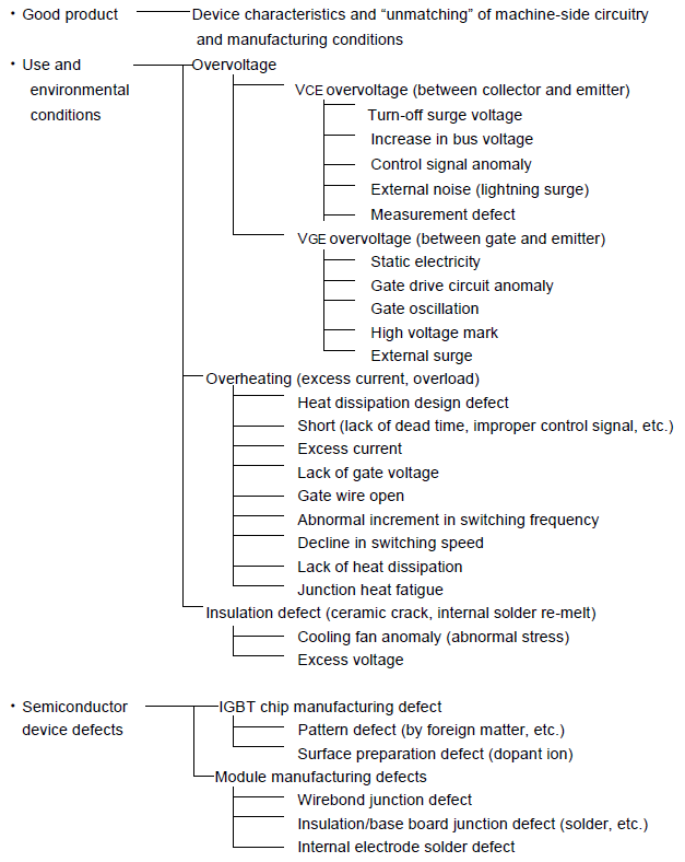
When a device is returned from the market or the equipment-assembly conditioning evaluation as faulty and a fault analysis is performed on a good product, there may be a problem with the device in use or the environmental conditions, or there may be a defect in the device. Using the IGBT module as an example, the fault factors are listed below:
Among the factors above, one of the factors deciding the usable life period is heat fatigue failure inside the module between the chip and wire junction or between the insulation substrate and the base plate (solder junction).
The quality, price, delivery and service of a product are all important elements but the most important thing as long as the product exists is the quality of the product and the continuing service to the user of the product.
In the semiconductor industry, the quality levels required by products are very high. On the other hand, high quality control is required in the mass-production systems with very advanced technology such as the process control capability seen in the "wafer process" or the minute work seen in the "assembly process".
A brief description of the quality-guaranteeing activities is given below.
3.1 Mass production procedures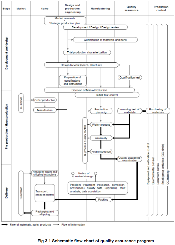
From trial production in development through trial mass production until mass production, a series of type approval tests are carried out for performance and reliability, along with an examination of a typical design illustration. Fig.3.1 shows a quality-guarantee system illustration from development through mass production.
The next chapter provides information on the reliability tests and reliability confirmation in the type-approval tests.
The next chapter provides information on the reliability tests and reliability confirmation in the type-approval tests.
3.2 Environmental control
In the semiconductor industry, the environment greatly effects product quality and control limits are established to control the environment precisely and monitor dust, moisture and temperature. The same measures are taken with the gas and water used in the factory.
3.3 Periodic inspection of manufacturing equipment, instrumentation and maintenance control
The semiconductor industry is a manufacturing industry and control of the manufacturing equipment and Instrumentation is important in device production. Regular checks and maintenance are performed to prevent any decline in accuracy, faults, etc., in the device.
3.4 Material purchasing control
Strict analysis and inspection are performed using spectrum analysis etc. based on receipt inspection norms. After sufficient sample examination has been performed to confirm the quality of the supplied materials and all problems solved, formal delivery begins. Due consideration is also given to the quality control of the supplier’s manufacturing process.
3.5 Manufacturing process control
The conditions that greatly influence quality control, such as purity of demineralized water atmosphere, furnace temperature, gas flow rate, etc., are measured by instruments mounted on the respective parts, automatically recorded and checked by engineers using check sheets. Moreover, processes that can have a larger effect on characteristics, such as depth of diffusion, surface concentration, etc. are recorded and used in the control data for working conditions. In addition, to assure stable quality, control is performed with data acquisition regarding the assembly processes which affect the wire-bond process’ adhesion pressure, strength control, etc.
3.6 Intermediate and final inspections
Our policy on intermediate and final inspections is thus: With the aim of measuring the reduction in variation and
improving the maintenance of quality, and thus producing better products, data on the product’s quality characteristics,
such as appearance, size, structure, and electrical characteristics, etc., are returned to the first manufacturing stage.
Intermediate inspections include wafer test and assembly process sampling inspections. All are carried out by two independent checks: one by the works section, based on the motto of "making quality from the manufacturing process", and one by the quality-control section. By correcting quality according to the independent checks, we are able to check on points that are hard to discover in the finished product. After product completion the final inspection is conducted as a finished-goods inspection. Finally, electrical properties and external appearance are inspected.
From the viewpoint of the customer who will use the product, to confirm the total performance and quality of the product, before the product is stored it is again sampled and subjected to quality guaranteeing inspections for external appearance, electrical characteristics and reliability. The quality of the warehouse is also strictly checked for each lot.
From the viewpoint of the customer who will use the product, to confirm the total performance and quality of the product, before the product is stored it is again sampled and subjected to quality guaranteeing inspections for external appearance, electrical characteristics and reliability. The quality of the warehouse is also strictly checked for each lot.
3.7 Quality information
Various data on quality, such as inspection results and customer information, is created mainly in the quality guaranteeing section, and is rapidly sent to the related section including a manufacturing department for the continued improvement of quality.
4.1 Reliability Test Method
Mitsubishi semiconductor devices can be used with full satisfaction because they are built to high levels of reliability: precise quality control through the design and manufacturing processes along with quality-guaranteeing inspections of every production lot assures high reliability. Various reliability tests are performed to check the level of reliability.
The example of the test item and test conditions for the representative type of power modules are shown below. Mitsubishi semiconductor devices are tested for reliability refer to Japan Electronics and Information Technology Industries Association (JEITA). (Related standard: International Electrotechnical Commission Standard( IEC standard)).
The example of the test item and test conditions for the representative type of power modules are shown below. Mitsubishi semiconductor devices are tested for reliability refer to Japan Electronics and Information Technology Industries Association (JEITA). (Related standard: International Electrotechnical Commission Standard( IEC standard)).
| Item | Conditions | |
|---|---|---|
| Environmental Testing | Thermal Shock | 100℃ : 5 minutes, 0℃ : 5 minutes, 10 cycles |
| Temperature Cycle | -40℃(60 minutes)~125℃(6 minutes), 10 cycles | |
| Vibration | 10~500Hz / 15 minutes, 10G, 6 hours | |
| Terminal Strength |
9.8~40N, 10±1 seconds 2.2±0.1N, 30 seconds |
|
| Soldering Thermostability |
[Condition A] 260℃, 10+2/-0 seconds、 or [Condition B] 270℃, 7+2/-0 seconds, or [Condition C] 350℃, 3.5±0.5 seconds |
|
| Solderbility |
[Condition A] 235±5℃, 5±0.5 seconds, or [Condition B] 245±5℃, 5±0.5 seconds |
|
| Mounting Strength |
M8 : 8.83~10.8N•m, 10±1 seconds M6 : 2.94~4.5N•m, 10±1 seconds M5 : 1.96~3.5N•m, 10±1 seconds M4 : 1.47~1.7N•m, 10±1 seconds M3 : 0.98N•m, 10±1 seconds |
|
| Endurance Testing | High Temperature Storage | Ta=125℃, 1000 hours |
| Low Temperature Storage | Ta=-40℃, 1000 hours | |
| Moisture Resistance |
[Condition A] Ta=60℃, RH=90%, 1000 hours or[Conditon B] Ta=85℃, RH=85%, 1000 hours |
|
| High Temperature Reverse Bias | Ta=125℃, VCE=max rating voltage×0.85 V, VGE=0V, 1000 hours | |
| High Temperature Gate Bias | Ta=125℃, VCE=0V, VGE=20V, 1000 hours | |
| Intermittent operating life | △TC=50℃ (△Tj=100℃), 5000 cycles | |
5.1 Heat stress model during module actuation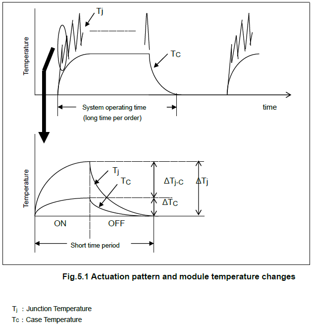
Two actuation patterns of the heat stress model during module actuation are shown in sections in Fig.5.1 When selecting a module, consideration must be given to its usable life and the machine design.
- ■Action mode 1
- Actuation pattern shows few changes in case temperature (base plate temperature) but frequent changes in junction temperature (known as PC life or power cycle life).
- ■Action Mode 2
- Actuation pattern shows relatively calm temperature changes at system actuation and shut down (known as thermal cycle life).
5.2 Fault mechanism with power cycle and thermal cycle
5.2.1 Power-cycle life fault mechanism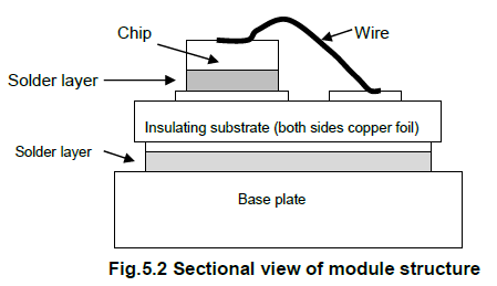
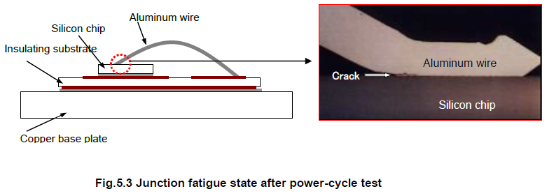
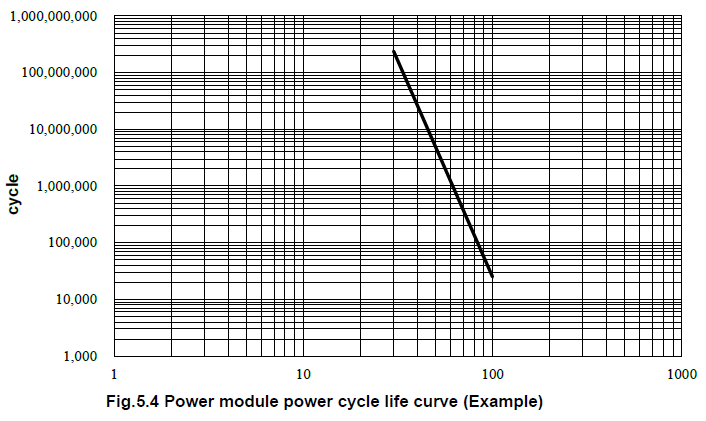
Fig. 5.2 shows the structure of a typical power module as module actuation causes a change in the junction temperature and stress appears by the difference in linear expansion coefficients of the aluminum wire and the silicon chip, causing a crack to appear on the junction side. The crack develops and eventually separates completely.
With the comparatively gentle changes in module-case temperature by inverter actuation, etc., when conditions cause frequent junction temperature changes, power cycle disruption must be taken into consideration during machine design. Fig. 5.3 shows a photograph of a case of junction shear due to power cycle.
Fig. 5.4 shows the results of our company’s test carried out on a module product’s power-cycle life (power cycle life curve).
5.2.2 Power-cycle life fault mechanism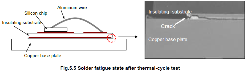
At system actuation and shutdown, the power module’s case temperature (Tc) changes comparatively gently while large temperature change occurs at actuation pattern, the stress distortion occurs in the solder layer caused by the difference in the thermal expansion coefficient between the base plate and the insulation substrate in Fig. 5.2.
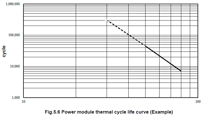
When this stress is repeated, a crack appears in the solder and when the crack reaches the bottom of the power chip, it causes increased thermal resistance and thermal disruption. Finally, due to the thermal resistance increase, the ΔTj increases and power-cycle proof decreases, and power cycle life reaches wire-shear mode. Fig. 5.5 shows a photograph of a solder layer crack between the insulation substrate and base plate caused by thermal cycle. Fig. 5.6 shows the results of a thermal-cycle life test on module products carried out by the company.
When this stress is repeated, a crack appears in the solder and when the crack reaches the bottom of the power chip, it causes increased thermal resistance and thermal disruption. Finally, due to the thermal resistance increase, the ΔTj increases and power-cycle proof decreases, and power cycle life reaches wire-shear mode. Fig. 5.5 shows a photograph of a solder layer crack between the insulation substrate and base plate caused by thermal cycle. Fig. 5.6 shows the results of a thermal-cycle life test on module products carried out by the company.
Power devices of the reliability test result are shown below.
| Product name | |
|---|---|
| IGBT modules T series NX type | |
| IGBT modules T series LV100 type | |
| HVIGBT modules X series | |
| Full SiC Super Mini DIPIPM | |
| FullSiC SLIMDIP | |
| SLIMDIP | |
| Super Mini DIPIPM Ver.7 | |
| Compact DIPIPM | |
| Mini DIPIPM Ver.7 | |
| Large DIPIPM Ver.6 | |
| Large DIPIPM+ | |
| Automotive IGBT modules J1 series |
Please contact our sales office for reliability test result of power module not listed here.
DIPIPM, SLIMDIP, DIPIPM+, SOPIPM and DIPPFC are trademarks of MITSUBISHI ELECTRIC CORPORATION.