

News
Note that the releases are accurate at the time of publication but may be subject to change without notice. This page shows only the most recent items. For the full archive of press releases please click "Search by category or year."
Mitsubishi Electric to Ship Samples of SiC-MOSFET Bare Die for xEVs
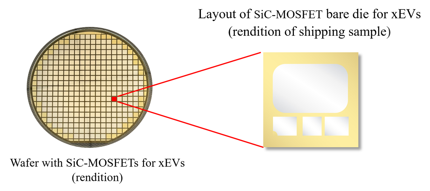
(left) Wafer with SiC-MOSFETs for xEVs (rendition) (right) Layout of SiC-MOSFET bare die for xEVs (rendition of shipping sample)Sub-nanosecond pulsed deep-ultraviolet laser system
TOKYO, November 12, 2024 - Mitsubishi Electric Corporation (TOKYO: 6503) announced today that it will begin shipping samples of a silicon carbide (SiC) metal-oxide-semiconductor field-effect transistor (MOSFET) bare die for use in drive-motor inverters of electric vehicles (EVs), plug-in hybrid vehicles (PHEVs) and other electric vehicles (xEVs) on November 14. Mitsubishi Electric's first standard-specification SiC-MOSFET power semiconductor chip will enable the company to respond to the diversification of inverters for xEVs and contribute to the growing popularity of these vehicles. The new SiC-MOSFET bare die for xEVs combines a proprietary chip structure and manufacturing technologies to contribute to decarbonization by enhancing inverter performance, extending driving range and improving energy efficiency in xEVs.
Mitsubishi Electric's new power semiconductor chip is a proprietary trench* SiC-MOSFET that reduces power loss by about 50% compared to conventional planar** SiC-MOSFETs. Thanks to proprietary manufacturing technologies, such as a gate oxide film process that suppresses fluctuations in power loss and on-resistance, the new chip achieves long-term stability to contribute to inverter durability and xEV performance.
* Groove (trench) is dug from the surface of the wafer and the gate electrode is embedded.
** Gate electrode is placed on the surface of the wafer.