


News
Note that the releases are accurate at the time of publication but may be subject to change without notice. This page shows only the most recent items. For the full archive of press releases please click "Search by category or year."
Mitsubishi Electric Achieves World’s First Demonstration of Suppression of Frequency Dispersion in GaN Transistors Using GaN Substrates
 PDF Version (PDF:797.0 KB)
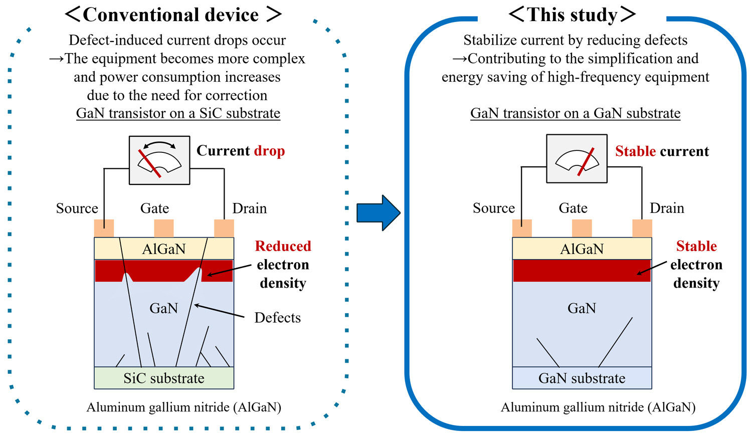
Comparison of crystal defects in GaN epitaxial layers on SiC and GaN substrates
TOKYO, November 9, 2026 – Mitsubishi Electric Corporation (TOKYO: 6503) announced today that it has, for the first time in the world,1 elucidated the effects of frequency dispersion2 caused by crystal defects in a gallium nitride (GaN) transistor, a high-frequency transistor fabricated by depositing a GaN epitaxial layer3 on a GaN substrate, and demonstrated that frequency dispersion can be significantly suppressed.
This achievement makes it possible to consistently realize the inherently high performance of GaN, contributing to the miniaturization, improved performance, and lower power consumption of high-frequency equipment, including industrial microwave heating systems that use GaN transistors.
In recent years, demand for high-power, high-efficiency GaN transistors has been rapidly increasing in high-frequency fields, including industrial microwave heating systems used for chemical recycling, which converts waste plastics back into chemical raw materials, as well as 5G/6G base stations and radar systems. Conventional GaN transistors have mainly been fabricated by forming a GaN epitaxial layer on a silicon carbide (SiC) substrate because SiC has high thermal conductivity and provides effective heat dissipation. However, crystal defects have been unavoidable during the film formation process due to the difference in materials between the substrate and the epitaxial layer.
These crystal defects impede the movement of electrons during high-frequency operation, causing frequency dispersion, in which current values vary depending on the frequency, and resulting in unstable device operation. Consequently, complex correction using digital circuits had previously been required, making increased overall system size and greater power losses significant challenges.
As part of a project commissioned by Japan’s Ministry of the Environment,4 Mitsubishi Electric has elucidated the effects of crystal defects on frequency dispersion through device characterization of GaN transistors incorporating GaN substrates,5 an area in which Japanese companies have particular strengths, using a new circuit analysis method that incorporates defect-related response.6
By demonstrating, for the first time in the world, that frequency dispersion can be significantly suppressed on a GaN substrate and that flat frequency characteristics can be obtained, Mitsubishi Electric has made it possible to simplify the digital correction circuits that had previously been essential. This will contribute to the miniaturization, improved performance, and lower power consumption of high-frequency equipment.
Details will be presented at the International Workshop on Nitride Semiconductors 2026 (IWN2026), to be held from November 8 to 13 at Kumamoto Castle Hall in Kumamoto City, Japan.
- 1
According to research conducted by Mitsubishi Electric on October 26, 2026; 156 research papers were identified through a Google ScholarTM search using the keywords “GaN substrate,” “GaN wafer,” and “GaN on GaN HEMT,” and then reviewed.
- 2
A phenomenon in which current values and other characteristics of high-frequency devices vary depending on the operating frequency.
- 3
A single-crystal layer grown on a single-crystal substrate.
- 4
Mitsubishi Electric has been participating since 2024 in the Project “Acceleration of Social Implementation and Dissemination of Components and Materials for Realizing Innovative CO2 Emission Reduction” by Ministry of the Environment, Japan and is conducting technological development related to high-efficiency GaN transistors.
- 5
Using a substrate made entirely of GaN that can be handled independently.
- 6
The electrical response or behavior exhibited by defects in a material in response to external stimuli.
Inquiry
-
Media contact
-
Customer Inquiries
Advanced Technology R&D Center
Mitsubishi Electric CorporationFax: +81-6-6497-7285